

Qingdian Photovoltaic - Monocrystalline Silicon Wafer Production Base
Release Date:2025-03-04 Source: Number of views:368
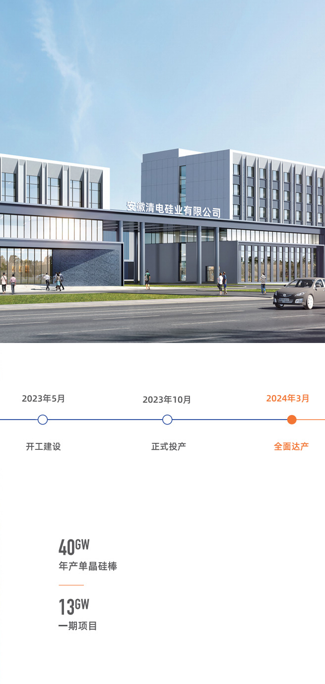
The first phase 13GW production base of Anhui Qingdian Silicon Industry Co., Ltd. with an annual output of 40GW monocrystalline silicon wafers is located in Hefei Circular Economy Demonstration Park. The project covers an area of about 150 acres, and the production workshop of the first phase project has 32 production lines and a total of 212 main equipment. It is the first fully intelligent slicing production line in the group's entire industry that integrates adhesive, slicing cleaning, and packaging. It can process ultra-thin full and half slice technology with edge distance of 230mm and thickness below 130um, which is far ahead.
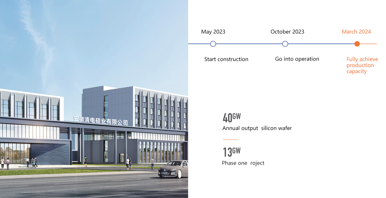
The first phase 13GW production base of Anhui Qingdian Silicon Industry Co., Ltd. with an annual output of 40GW monocrystalline silicon wafers is located in Hefei Circular Economy Demonstration Park. The project covers an area of about 150 acres, and the production workshop of the first phase project has 32 production lines and a total of 212 main equipment. It is the first fully intelligent slicing production line in the group's entire industry that integrates adhesive, slicing cleaning, and packaging. It can process ultra-thin full and half slice technology with edge distance of 230mm and thickness below 130um, which is far ahead.